
You might be wondering how a shark could be related to the surface roughness topic? As a child, I always thought animals have teeth similar to human beings until I watched the deep blue sea movie. Similarly, I always thought that copper foils and metallic surfaces are quite smooth in nature until I learned the nuances of the copper foil manufacturing process. We will discuss in this topic of how the shark-like teeth of copper (surface roughness) impacts the signal integrity performance.
Surface roughness is a concept that we see at least one DesignCon paper every year. I am expecting the coming DesignCon conferences no different. Upon deeper review of these topics, we will find that they are loaded with mathematical models as well as complicated jargons such as cannon ball model, profilometer measurements and SEM scanning, which makes all of these topics sound like a PHD research topic.
In the end, everything boils down to the following discussion: Is the copper foil a smooth surface or a rough surface. If it is a rough surface, how rough it is and what is the deviation of that roughness from what is considered being smooth ? Why do we need to understand this topic?
The total loss is characterized in the following way:
Total Loss = Insertion Loss of Dielectric + (Surface roughness coefficient * Insertion Loss of conductor)
Let us understand why a copper will introduce loss into the signal. To understand this, let us first discuss what is skin effect and why the currents will flow outside the conductor.
Skin Effect and Skin Depth:
The skin effect is a phenomenon whereby alternating electric current does not flow uniformly with respect to the cross-section of a conductive element, such as a wire [1].
The current density is highest near the surface of the conductor and decreases exponentially as distance from the surface increases. Skin depth is a measure of how far electrical conduction takes place in a conductor, and is a function of frequency. At DC (0 Hz) the entire conductor is used, no matter how thick it is. At microwave frequencies, the conduction takes place at the top surface only. As we go down the surface, the current density decrease. This can be seen even in the animation presented below.

Eddy Currents and Magnetic Fields:
When a good electrical conductor (like copper or aluminum) is exposed to a changing magnetic field, a current is induced in the metal, commonly called an eddy current. Eddy currents flow in closed loops within conductors, in planes perpendicular to the magnetic field.

Why is Copper Foil roughened?
Copper foil is roughened to promote adhesion of the dielectric resin to the conductor in printed circuit boards. Adhesion at the interface between conductor and insulator must be very robust due to conditions during manufacturing, assembly, and standard usage to which a printed circuit board is subjected. This interface is exposed to corrosive chemicals during processing and to high temperature, high humidity, cold, shock, vibration, and shear stresses during use. Technologies that optimize surface and resin chemistries, as well as surface area, are utilized by foil manufacturers and laminators to promote and retain adhesion.

As shown in the Figure3 ( Reference [1]), the 90° peel strength is a measure of how well a conductor adheres to the dielectric material and is directly proportional to the fourth root of the thickness of deformed resin (yo) and other parameters like foil thickness, etc. The adhesive interlayer thickness is correlated to the treatment height. Higher roughness increases the interlayer thickness, the surface area, and the chemical contributions to peel strength. Though roughness contributes positively to peel, it has a negative impact on signal integrity.
Copper Foil Manufacturing Process:
There are various ways of copper foil manufacturing process available in PCB industry. Electro-deposited (ED) copper is widely used in the PCB industry. A finished sheet of ED copper foil has a matte side and drum side. The drum side is always smoother than the matte side.

The matte side is usually attached to the core laminate. For high frequency boards, sometimes the drum side of the foil is laminated to the core. In this case it is referred to as reversed treated (RT) foil. Various foil manufacturers offer ED copper foils with varying degrees of roughness. Each supplier tends to market their product with their own brand name. Presently, there seems to be three distinct classes of copper foil roughness:

Some other common names referring to ULP class are HVLP or eVLP. Profilometers are often used to quantify the roughness tooth profile of electro-deposited copper. Tooth profiles are typically reported in terms of 10-point mean roughness (Rz ) for both sides, but sometimes the drum side reports average roughness (Ra ) in manufacturers’ data sheets. Some manufacturers also report RMS roughness (Rq ). Now we know why we have roughness in the copper profile.
Simulation vs Measurement (Chicken and Egg Story)
It is quite tough to interpret the manufacturer’s data sheet. Some authors argue to use design feedback methodology.
Design a test coupon –>fabricate the board –> Measure the frequency domain parameters performance –>Extract the Dk,Df and surface roughness of the board –> Cross Verify and compare against the simulated parameters –> 100% it will vary –> Now add back into the simulation channel performance –>Re simulate the analysis ! This is called Design feedback methodology. In a competitive cut throat market this is time consuming procedure. Money and resources go for a kick !Consider the analysis demonstrated in Fig 6 and 7, we can observe two different set of designs. Figure 6 consists of measured calibration traces of the same design and same manufacturer and So is with Figure 7 analysis
Which sample should we consider for measuring the material parameters? To solve this issue to certain extent, empirical models will allow us to reach our goal sooner. I always used to listen this statement from my manager: Sometimes an OK answer NOW is better than a good answer. This statement is made by Eric Bogatin.

Empirical Models: Surface Roughness Coefficient
Calculating the surface roughness coefficient is done via an empirical model fit. Finding the right empirical fit to the measured data is the ball game in the research papers and the tussle to be better than previous used models.
Empirical Models that are available in market for calculating the surface roughness of the conductors:
1) Morgan – Hammerstad 2) Groisse Model 3) Huray “Snowball” 4) Hemispherical model (Hall, Pytel) 5) Stochastic models (Sanderson, Tsang). May be there could be more than mentioned but I restricted the analysis for the first three models.
There is one more advanced model developed by Bert Simonvich based on Huray Snowball. Polar instruments has implemented this model in their software. If you want to learn more, all his application notes are sufficient to understand the analysis [4].
Also, I want to mention about Yuriy Shlepnev, Simberian Inc application notes regarding this topic. The following paper : Conductor surface roughness modeling: From “snowballs” to “cannonballs” discusses in detail about the myth surrounding the models [5]
Morgan -Hammerstad:
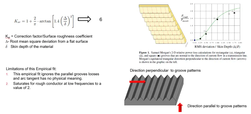
Power absorption factor Ksr is defined as ratio of power dissipated by the eddy currents in a conductor per unit area when the surface is rough, Pa,rough, to the power dissipated when the surface is smooth, Pa,smooth. Consider the formulation no 4 and 5 which are interpreted as per above discussion.

Ksr is used as a correction factor to account for the conductor surface roughness effect when calculating attenuation. The attenuation constant, αc,rough, for wave propagation in waveguides involving conductors with rough surfaces can be estimated by multiplying the attenuation constant calculated for a smooth conductor, αc,smooth, with Ksr.
Samuel Morgan: Reference Paper -[2]
Highlights of research paper: Morgan determined that, at 10 GHz, current flow transverse to periodic structures could increase loss by up to 100%! If the current flow was parallel, the losses increased by up to 33%. Morgan hypothesized the cause for this additional loss assumed that the loss was a function of the RMS distortion of a rough surface relative to the electromagnetic skin depth of a perfectly smooth metal surface with conductivity equal to that of the bulk metal.
In the paper, Morgan experimented the analysis on equilateral, triangular and square shapes and considered the cases to be treated as two dimensional; the surface roughness is assumed to consist of infinitely long parallel grooves or scratches either normal to or parallel to the direction of induced current flow. From the analysis, Morgan figured out that transverse grooves have a considerably greater adverse effect than grooves parallel to the current.

Morgan -Hammerstad Empirical Fit:
In 1975, Hammerstad proposed an empirical fit for the Morgan’s published data and it was is quite ok at that time, however it saturates for the rough conductor at low frequencies to a value of 2.
As observed in the results, the empirical fit is very limited and hence advised not to use this method for validating the copper profile roughness.
Groisse Model (Available in the ANSYS Software):
I would give a very brief analysis about this model. This model is slightly better than Hammerstad model. However even this model saturates to a value of 2. The symbols used in the equation holds the same as explained earlier. This model is seldom used at our end.

Huray Model (Snow Ball Model):
Before we move into this model, there are few insights Paul.G.Huray provided along with the other authors in this paper. I wish all SI engineers read this reference paper without fail. It is quite lengthy and may take time but worth a read.
Does surface roughness increase the length and resistance ? Does the current take longer time to travel in case of rough surface ? Actually the answer is NO. In case you felt yes, then the propagation delay should have been increased in case of rough copper surface.

Let us understand what does this author means: The answer is that local surface charge density (Quantity of charge per unit area) is formed by the displacement of conduction electrons transverse to the surface profile so that a wave of charge density propagates at whatever speed is needed to support the external electric field intensity in the transmission line. No charged particles actually move at relativistic speeds ( a speed comparable to speed of light).
A current flowing on the rough surface of a conductor cannot be regarded as a current flowing on a flat surface of the conductor with a longer equivalent path. When current flows in a conductor, assuming that the current distribution decays exponentially within the depth of the conductor, the model is not correct either.
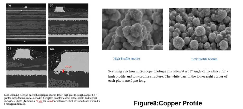
As discussed earlier, high profile samples resemble copper nodule pyramid structures arranged in a nominal hexagonal pattern on a matte finish surface. By comparison, the low profile samples appear to be made up of similar size copper nodules randomly scattered on a flat plane; the nodules vary in radius but the average size is about 1 μm in diameter.
Now let us come back to the empirical model developed by Paul Huray, we shall neglect the non uniform model architecture developed by the team as it does not contribute much but gave a pathway to develop EDA based empirical model.
Uniform Snowball Architecture:


So now that the Huray Model equation is understood, the next task is how to fit these complicated equations into the EDA toolkit. Below is the simulation analysis for various empirical model fits.


What do I do in my daily life simulation and measurement analysis:
Get from the vendor (TTM/Sanmina/Founder) the data sheet of the dielectric materials being used in the stack up design. It could be either MEG 6 or MEG 7 or Tachyon 100 G and obtain the surface roughness measurement value (eg Rz) which is roughly divided into low/medium/high roughness, understand the roughness difference between the top surface and the bottom surface, and apply all of them into the simulation model. For Dk and Df fit, I use Djordjevic-Sarkar model (Wide Debye Model). Then use the design feedback methodology.
That’s all Amigos ! This took really a lot of time as I went back and forth to understand. Next time, when you see the canon ball or surface roughness as topic at DesignCon, you will be more educated on this topic 😉
Thanks for reading, I hope you enjoyed reading this discussion.
References:
1) Non-Classical Conductor Losses due to Copper Foil Roughness and Treatment by Gary Brist and Stephen Hall Intel Corporation Hillsboro, Sidney Clouser, Tao Liang
2)S.P. Morgan Jr., “Effect of Surface Roughness on Eddy Current Losses at Microwave Frequencies,” Journal of Applied Physics, Vol. 20, p. 352-362, April 1949.
3) Practical methodology for analyzing the effect of conductor roughness on signal losses and dispersion in interconnects.
4)Simonovich, Bert, “Practical Method for Modeling Conductor Surface Roughness Using The Cannonball Stack Principle”, White Paper.
5)Conductor surface roughness modelling: From “snowballs” to “cannonballs” Yuriy Shlepnev, Simberian Inc.
Written by: Kalyan Vaddagiri
Senior SI Engineer at Molex
Original Article on LinkedIn


